Certificate of Competency (CRI 4.0) - Certified by Centre For Research In Industry 4.0 (CRI 4.0), University Malaya.
This course introduces learners to the full custom IC design flow including specification, schematic capture, layout, simulation, verification, and physical design. Participants will gain exposure to both analog and digital IC design techniques with a focus on CMOS technologies. The course emphasizes practical design using EDA tools like Cadence, Synopsys, or open-source platforms such as OpenROAD and Magic VLSI. Students will undertake a mini-project involving the design, layout, and verification of a simple IC block.
The course aims to provide a comprehensive understanding of the methodologies, tools, and techniques involved in the design and fabrication of custom Integrated Circuits (ICs). It bridges theoretical microelectronics knowledge with hands-on design skills using industry-standard Electronic Design Automation (EDA) tools.
The course develops specialized skills in:
Learning Outcome
Who Should Take This Course?
This course is ideal for diploma and degree holders in Electronics, Electrical, or Electronics & Communication Engineering who are looking to build expertise in semiconductor technologies. It is also well-suited for professionals aiming to specialize in VLSI, ASIC, SoC, or FPGA domains, as well as research scholars pursuing advanced studies in microelectronics or semiconductor engineering.
Pre-requisite
To ensure participants can fully benefit from the course, the following background is recommended:
-
Academic: A minimum qualification of a diploma in
Electronics, Electrical, or a
closely related engineering discipline.
-
Technical Knowledge: A basic understanding of semiconductor
physics, circuit
theory, and digital logic design is essential.
-
Tool Familiarity: Prior exposure to circuit simulation
tools such as SPICE is
beneficial, though not mandatory for enrollment.
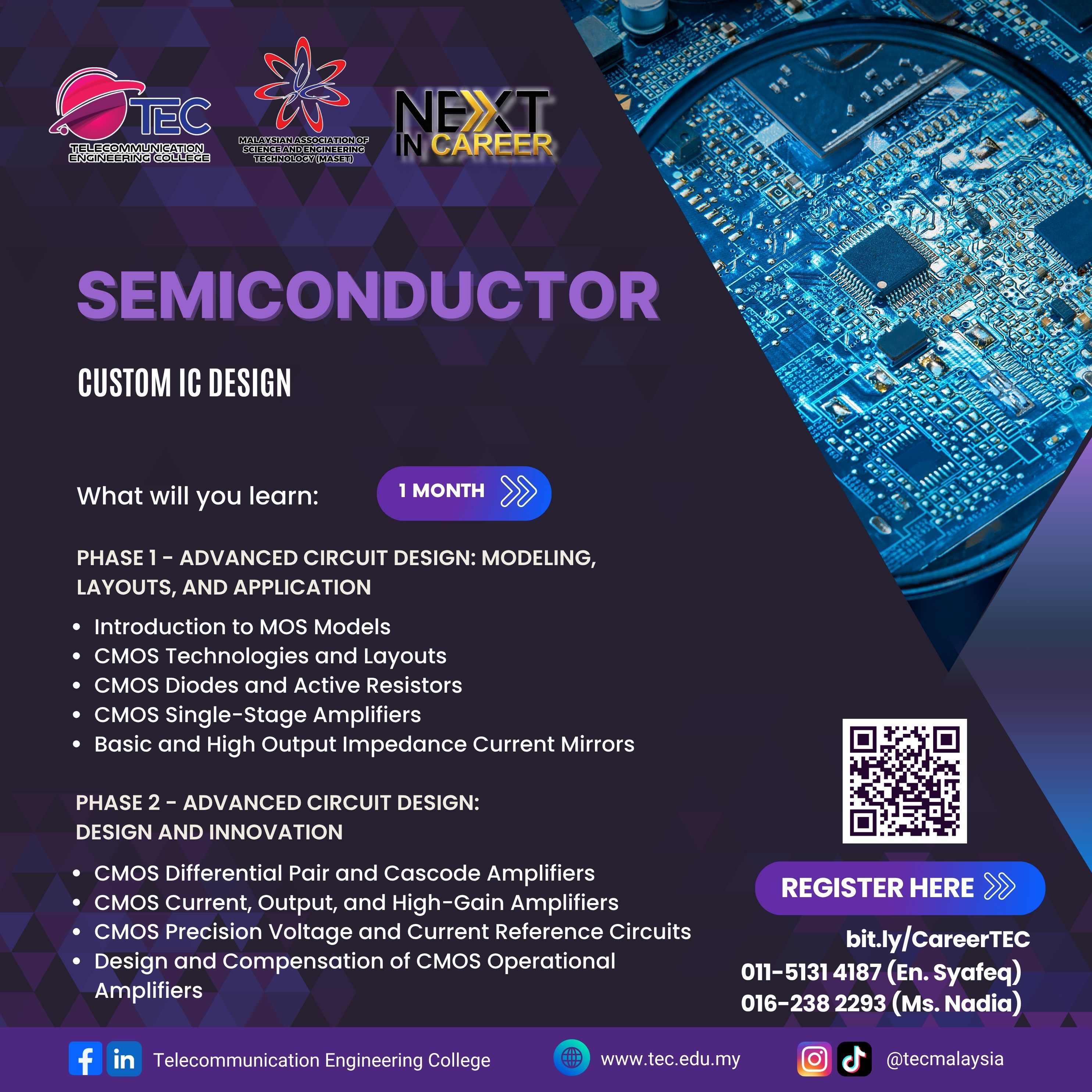
CHAPTER 2 – CMOS Technologies and Layouts
CHAPTER 4 – CMOS Single-Stage Amplifiers
CHAPTER 5 – Basic and High Output Impedance Current Mirrors
CHAPTER 6 – CMOS Differential Pair and Cascode Amplifiers
CHAPTER 7 – CMOS Current, Output, and High-Gain Amplifiers
CHAPTER 8 – CMOS Precision Voltage and Current Reference Circuits
CHAPTER 9 – Design and Compensation of CMOS Operational Amplifiers
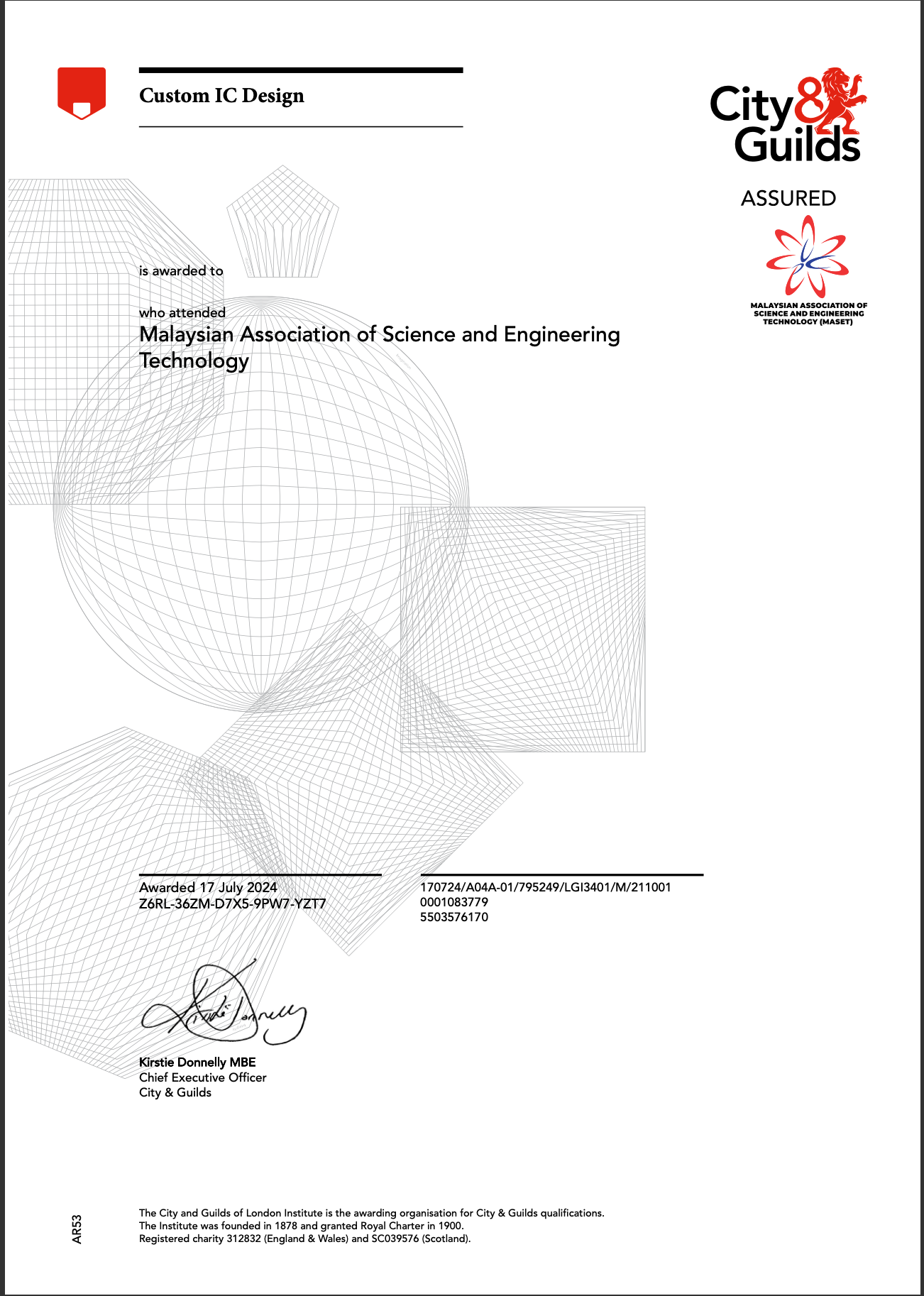
Upon successfully passing the examination for this course, participants will be awarded a certificate, an example of which is shown below.
Semiconductor (Custom IC Design)